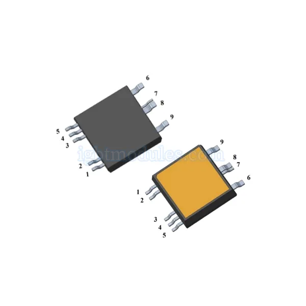
1. SiC Material Advantages
BYD Microelectronics SiC MOSFETs use silicon carbide, a wide bandgap semiconductor material that enables superior performance versus silicon in high voltage and high frequency applications.
Material Properties
• Wide bandgap of 3.26eV; High critical electric field; High thermal conductivity; Low intrinsic carrier concentration; High electron saturation velocity
Device Benefits
• Lower Rds(on) per area; Higher operating temperature; Faster switching transitions; Lower switching losses; No tail current during turn-off
2. SiC MOSFET Product Architecture
BYD SiC MOSFETs are designed for 1200V and 1700V platforms, targeting applications where silicon IGBTs or superjunction MOSFETs face performance limits.
Device Configurations
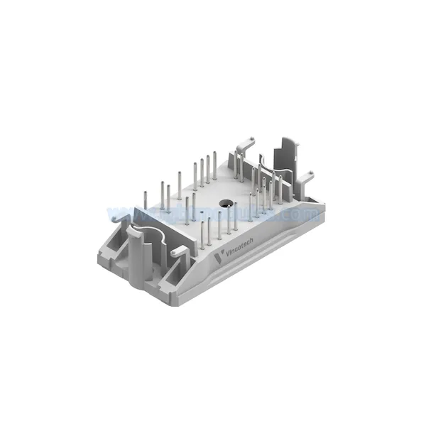
• Discrete SiC MOSFET in TO-247; SiC MOSFET bare die; Co-packed with SiC SBD; Half-bridge module packages; Bare chip for custom integration
Key Electrical Features
• 1200V-1700V breakdown voltage; Low Rds(on) at high temperature; Fast body diode or co-packed SBD; Avalanche ruggedness; Gate drive compatible with SiC
| Platform | Voltage | Rds(on) Range | Package | Key Application |
|---|---|---|---|---|
| 1200V SiC | 1200V | 20-80 mohm | TO-247 | EV inverter, PFC |
| 1700V SiC | 1700V | 30-120 mohm | TO-247/Module | Industrial, traction |
| 1200V Module | 1200V | Custom | Module | High power EV |
3. Application Areas
BYD SiC MOSFETs address high efficiency power conversion applications where switching loss reduction enables smaller passive components and better thermal performance.
EV Power Electronics
• Traction inverter main switches; On-board charger DC-DC; Off-board DC fast charging; EV auxiliary power; 800V battery architecture support
Industrial and Energy
• Photovoltaic string inverters; Energy storage PCS; Industrial motor drives; Server and data center power; HVAC variable frequency drives
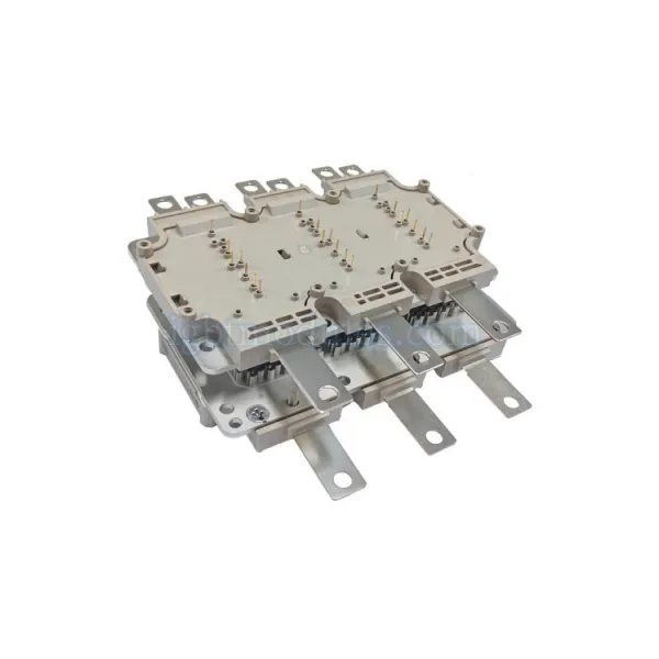
4. Design and Drive Considerations
SiC MOSFETs require careful attention to gate drive design, layout, and thermal management to fully leverage their performance advantages.
Gate Drive Requirements
• Higher gate drive voltage than Si MOSFET; Low gate resistance for fast switching; Kelvin source connection for clean drive; Isolated gate driver with high CMTI; Short dead-time management
Layout and Protection
• Low inductance power loop; Gate loop separate from power loop; dv/dt immunity of gate driver; Over-current protection; Short-circuit detection within 2us
FAQ
1:What are the key advantages of SiC MOSFETs over silicon IGBTs?
SiC MOSFETs offer lower switching losses due to no tail current during turn-off, lower Rds(on) at high temperature enabling better thermal performance, higher operating frequency for smaller passive components, and higher breakdown voltage per unit area. This translates to higher efficiency and power density.
2:What voltage platforms do BYD SiC MOSFETs target?
BYD SiC MOSFETs target 1200V and 1700V platforms. The 1200V platform is most common for EV traction inverters, on-board chargers, and PV inverters. The 1700V platform addresses higher voltage industrial and traction applications.
3:What gate drive considerations are important for SiC MOSFETs?
SiC MOSFETs typically require higher gate drive voltage (15-20V) than standard Si MOSFETs, low gate resistance for fast switching transitions, Kelvin source connection to reduce gate loop inductance, isolated gate drivers with high CMTI rating, and careful dead-time management to avoid shoot-through.