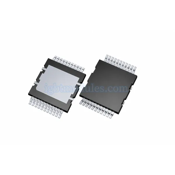
1. Superjunction Technology
BYD Microelectronics superjunction MOSFETs use a vertical structure with alternating p and n columns to overcome the silicon limit tradeoff between breakdown voltage and on-resistance.
Structural Advantages
• Deep p-n column structure; Reduced drift region resistance; Higher breakdown voltage at low Rds(on); Smaller die area for same voltage; Lower gate charge and capacitance
Performance Benefits
• Lower conduction losses; Higher efficiency at light load; Faster switching capability; Reduced switching losses; Improved power density
2. Voltage and Package Options
BYD superjunction MOSFETs target high voltage applications typically from 500V to 900V breakdown ratings.
Voltage Platforms
• 600V for universal AC PFC; 650V for improved margin; 700V-800V for higher reliability; 900V for specialized applications; Consistent voltage platform across packages
Package Selection
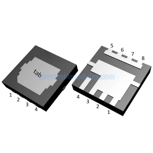
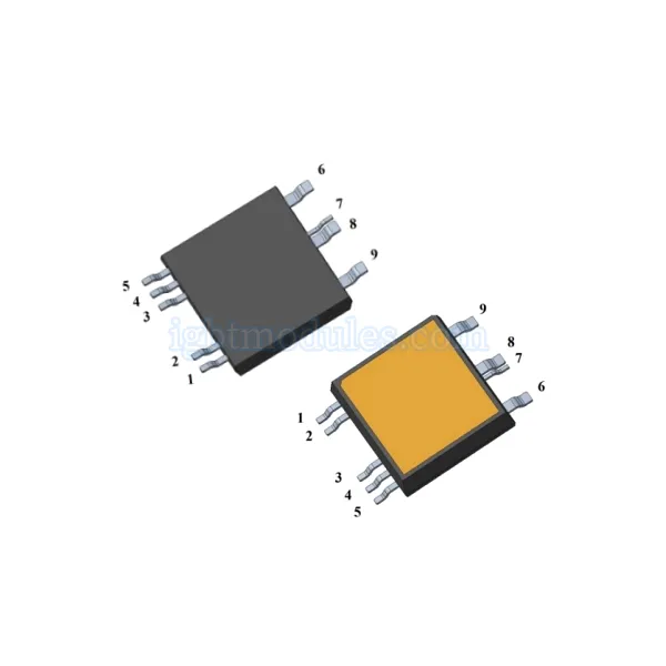
• TO-247 for high power; TO-220 for general purpose; TO-252 DPAK for surface mount; TO-263 D2PAK for higher power SMD; Bare die for integration
| Voltage Rating | Typical Application | Rds(on) Range | Package | Frequency |
|---|---|---|---|---|
| 600V | PFC stage | 0.1-1.0 ohm | TO-220/TO-247 | 50-200kHz |
| 650V | Adapter, PFC | 0.08-0.8 ohm | TO-220/DPAK | 50-200kHz |
| 700V | Industrial power | 0.15-1.5 ohm | TO-247 | 50-150kHz |
| 800V | EV charging | 0.2-2.0 ohm | TO-247 | 50-100kHz |
3. Power Supply Applications
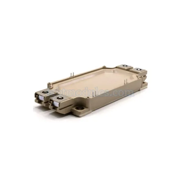
BYD superjunction MOSFETs are optimized for switch-mode power supply topologies where low switching loss and high voltage capability are critical.
SMPS Topologies
• Active PFC boost converters; LLC resonant half-bridge; Forward and flyback converters; Synchronous rectification; Hard switching PWM converters
Target Markets
• AC-DC adapter and charger; Server and telecom power; LED driver power supplies; Industrial power supplies; New energy PV micro-inverters
4. Design Considerations
When designing with BYD superjunction MOSFETs, consider gate drive, layout parasitics, and thermal management for optimal performance.
Key Design Factors
• Gate drive voltage and current; Layout inductance for switching speed; dv/dt immunity and noise; Heatsink thermal resistance; Avalanche energy capability
FAQ
1:What is the advantage of superjunction MOSFET technology?
Superjunction technology uses alternating vertical p and n columns to break the silicon limit tradeoff between breakdown voltage and on-resistance. This allows higher voltage ratings with lower Rds(on) compared to conventional planar MOSFETs, resulting in smaller die area, lower capacitance, and improved efficiency.
2:What voltage ratings are available for BYD superjunction MOSFETs?
BYD superjunction MOSFETs are typically available in 600V, 650V, 700V, and 800V-900V breakdown ratings. The 650V platform is most common for universal input PFC and adapter applications, while higher ratings address industrial and EV charging systems.
3:What switching frequency range suits superjunction MOSFETs?
BYD superjunction MOSFETs are typically used in the 50kHz to 200kHz range, with the optimal frequency depending on the specific topology, load condition, and thermal budget. LLC resonant converters may operate at higher frequencies while hard-switched PWM converters favor the lower end.