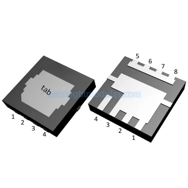
1. Materials and Dielectric Strength
- SGT MOSFET: Silicon-based device with a typical voltage rating of 30V–200V, suitable for low-voltage, high-current applications.
- SiC MOSFET: Wide-bandgap semiconductor with a voltage rating of 600V–3300V+, suitable for high-voltage applications.
2. Conduction and Switching Characteristics
- SGT MOSFET: Low on-resistance and fast switching speed, but reverse recovery losses in the body diode are significant.
- SiC MOSFET: Significant improvement in on-resistance per unit area as the breakdown voltage increases; extremely fast switching speed, with reverse recovery losses in the body diode being virtually negligible, making it suitable for high-frequency hard switching.
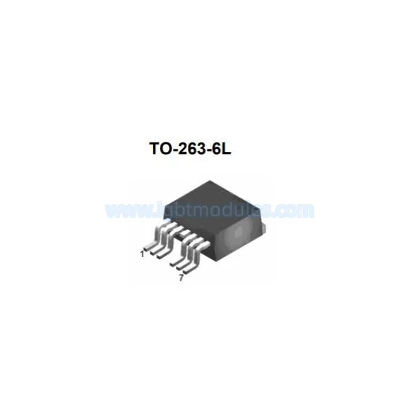
3. High Temperatures and Heat Dissipation
- SGT MOSFET: Junction temperature typically ranges from 150°C to 175°C; Rds(on) increases significantly at high temperatures.
- SiC MOSFET: Can operate at temperatures of 200°C and above; on-resistance changes minimally at high temperatures, offers higher thermal conductivity, and allows for a more compact thermal design.
4. Drivers and Costs
- SGT MOSFET: Simple to drive (10–12 V), low cost, and a mature supply chain.
- SiC MOSFET: Requires a dedicated driver (18–20 V negative voltage turn-off), is expensive (approximately 3–10 times that of silicon-based MOSFETs), but some of the cost can be offset at the system level (thermal management, magnetic components).
5. Typical Applications
- SGT MOSFET: DC-DC synchronous rectification, server power supplies, battery protection, motor drives (low voltage), and low-voltage automotive systems.
- SiC MOSFET: New energy vehicle main drive/OBC, photovoltaic inverters, energy storage PCS, charging stations, industrial high-voltage power supplies, and rail transit.
- Summary: SGT MOSFETs are the “best value for money” among silicon-based low-voltage, high-efficiency switches; SiC MOSFETs represent the “performance ceiling” for high-voltage, high-frequency, and high-temperature applications. The choice between them depends on voltage ratings, frequency, thermal management, and cost constraints.
Frequently Asked Questions
What is an SGT MOSFET?
- SGT MOSFETs and SiC MOSFETs are two types of power devices that differ completely in both operating principles and materials. Simply put, SGT MOSFETs are silicon-based devices that rely on structural innovations to enhance performance, while SiC MOSFETs are wide-bandgap semiconductor devices that leverage the advantages of their material.
- SGT MOSFET (Shielded-Gate Trench MOSFET)
This is an improved trench-structure device based on silicon. It features a shielded gate (polysilicon field plate) connected to the source, added beneath the gate of a traditional trench MOSFET.
- Core Principle: The function of this shielding gate is to shield the capacitive coupling between the gate and the drain. It can significantly reduce the “gate-drain capacitance” (patent data indicates a reduction of approximately 50%), thereby substantially reducing switching losses and enabling the device to operate at higher frequencies.
- Performance Features: In addition to fast switching, it utilizes the charge-balancing effect to reduce on-resistance while maintaining breakdown voltage. Therefore, it is ideally suited for applications requiring low power consumption and high frequencies.
- Market Positioning: Primarily targeting low-voltage applications ranging from 25V to 200V, it serves as a key component in server power supplies, DC-DC converters, and battery protection circuits.
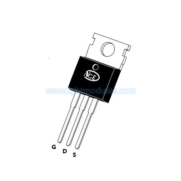
What is a SiC MOSFET?
- A MOSFET made from silicon carbide, a wide-bandgap semiconductor material. Its advantages stem directly from the physical properties of the material itself.
- Material Advantages: Silicon carbide has a much higher critical breakdown field strength than silicon, allowing devices to be designed with very high voltage ratings (commercial products range from 650 V to 15 kV). Additionally, it has higher thermal conductivity, enabling stable operation at higher temperatures, extremely fast switching speeds, and virtually negligible reverse recovery losses.
- Technical Challenges: Despite its excellent performance, the reliability of the gate oxide layer and its high cost are key issues that need to be addressed in current manufacturing and applications.
- Market Positioning: Primarily targeting high-voltage, high-frequency, and high-temperature applications, such as main drive inverters for new energy vehicles, on-board chargers (OBCs), photovoltaic inverters, and energy storage converters.