Accelerating IGBT Module Development with 3D CAD
Speeding up the electro-magnetic module design for maximum chip performance utilization and robustness requires advanced tools for bond wire routing and electromagnetic simulations. SwissSEM published its approach in Bodo’s Power Systems Magazine, detailing how 3D bond wire modelling accelerates IGBT module development.
Creating Bond Wire Layouts Using 3D CAD
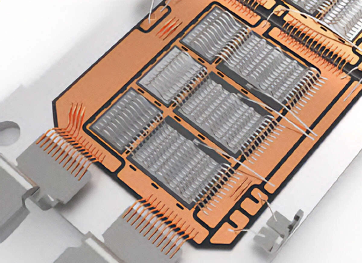
Although 3D CAD systems are well established in power module development for virtual prototyping and product documentation, bond wires are often missing in 3D models. While a single bond wire can be modelled with arcs and lines, modelling a complete bond wire layout is time-consuming since each wire has individual geometry.
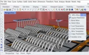
To address this, the software MFis Wire was released in 2020 by MFis GmbH, a company providing engineering services and tools focused on power electronics packaging.
MFis Wire Key Features
- User-friendly interface for 3D modelling of wedge, ribbon, and ball bond wires
- Bond wire drawn by selecting start and end point, then interactively defining loop shape and foot rotation
- Standard CAD commands: copy, move, mirror, array for modifying single or multiple bond wires
- Implemented as a plug-in for Rhino3D CAD platform
- Export to industry-standard CAD formats or conversion to 2D drawings with bond point coordinates
Geometry Optimization for Parasitic Extraction
The wire cross-sectional geometry must be chosen differently depending on the targeted use:
| Cross-Section Type | Best For | Advantages |
|---|---|---|
| Circular | Documentation, rendering | Natural appearance, low file size |
| Triangular | Electro-thermal FEA | Same cross-sectional area, efficient meshing |
| Hexagonal | Parasitic extraction | Balance of computing time and accuracy |
Case Study: ED-Type Module Optimization
Bond wire geometry modelling and parasitic extraction was performed for the ED-type module with a layout consisting of 165 wires connecting 661 points. Wires were exported in circular and hexagonal cross-section variants and processed using Ansys Q3D.
Performance Comparison
| Metric | Circular Cross-Section | Hexagonal Cross-Section |
|---|---|---|
| Convergence Time | 5.5 hours | 71 minutes |
| Memory Consumption | 22.3 GB | 11.4 GB |
| Self-Inductance Difference | Only 0.1% difference between variants | |
Design Optimization Results
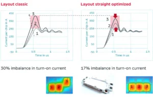
The ED-type module (industry standard 17mm height, 62 x 152mm IGBT module) presents challenges for internal current sharing between IGBTs due to its longish design. Through MFis Wire-enabled electromagnetic simulations, significant improvements were achieved:
- Current imbalance reduced from 30% to 17%, nearly a factor of two improvement
- Optimized layout through gate-position rotation and main emitter wire optimization
- Better load balancing within IGBTs
- Higher safe operating area utilization of IGBT chips
Conclusion
Simulation tools for thermal and electro-magnetic simulations shorten development time and improve IGBT module design quality. By using MFis Wire software, time for creating complex 3D geometry models of bond wire layouts is significantly reduced. Using hexagonal wire cross-section in parasitic extractor input geometry results in four times faster computation, making it possible to investigate several layout variants in a single workday.
This method enabled an improvement of the ED-type module internal current sharing by nearly a factor of two compared to classic design approaches.