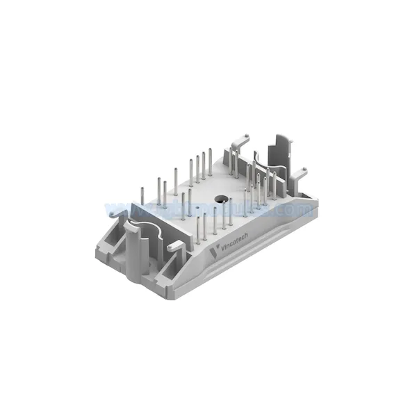

1. Physical Properties and Characteristics of SiC Materials
SiC (Silicon Carbide) is a compound semiconductor material composed of Si (silicon) and C (carbon). The critical breakdown field strength of SiC is 10 times that of Si, its band gap is 3 times that of Si, and its thermal conductivity is 3 times that of Si. Therefore, it is considered a power device material that surpasses the limits of Si.
Various polytypes exist in SiC, and their physical property values also differ. Among them, 4H-SiC is most suitable for power device fabrication. In addition, SiC is the only compound semiconductor that can form SiO2 through thermal oxidation, making it suitable for preparing MOS-type power devices.
2. Characteristics of Power Devices
Since the critical breakdown field strength of SiC is 10 times that of Si, compared with Si devices, high-voltage power devices can be fabricated with drift layers having higher impurity concentration and thinner thickness. The on-resistance of high-voltage power devices mainly comes from the drift layer resistance. Therefore, using SiC can achieve high-voltage devices with very low on-resistance per unit area. Theoretically, for devices with the same voltage rating, the drift layer resistance per unit area of SiC can be reduced to 1/300 of Si.
In Si materials, to address the problem of increased on-resistance accompanying higher voltage ratings, minority carrier devices (bipolar devices) such as IGBT (Insulated Gate Bipolar Transistor) are mainly used. However, they have the problem of large switching losses. As a result, the heat generated thereby limits the high-frequency driving of IGBTs.
SiC materials can achieve high voltage withstand with majority carrier devices (Schottky barrier diodes and MOSFETs) of high-frequency device structure, thereby simultaneously realizing the three characteristics of “high voltage withstand,” “low on-resistance,” and “high frequency.” In addition, the band gap is wider, 3 times that of Si, so SiC power devices can operate stably even at high temperatures.
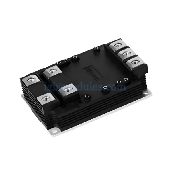
3. CRRC Characteristics of SiC MOSFET
3.1 Device Structure and Characteristics
In Si materials, the higher the voltage rating of the device, the larger the on-resistance per unit area (increases at approximately the 2.0 to 2.5 power of the voltage rating). Therefore, IGBTs (Insulated Gate Bipolar Transistors) are mainly used for voltages above 600V. IGBTs inject holes as minority carriers into the drift layer through conductivity modulation, so the on-resistance is lower than that of MOSFETs. However, at the same time, due to the accumulation of minority carriers, a tail current is generated during turn-off, resulting in significant switching losses.
SiC devices have lower drift layer resistance than Si devices. They can achieve high voltage withstand and low on-resistance with MOSFETs without requiring conductivity modulation. Moreover, MOSFETs theoretically do not generate tail current. Therefore, when replacing IGBTs with SiC MOSFETs, switching losses can be significantly reduced, and miniaturization of heat dissipation components can be achieved. In addition, SiC MOSFETs can be driven under high-frequency conditions where IGBTs cannot operate, which also enables miniaturization of passive components.
Compared with 600V to 900V Si MOSFETs, SiC MOSFETs have the advantages of small chip area (enabling small packages) and very low recovery loss of the body diode. They are mainly used in industrial machine power supplies, inverters or converters for high-efficiency power conditioners.
3.2 Normalized On-Resistance
The dielectric breakdown field strength of SiC is 10 times that of Si, so high voltage withstand can be achieved with a low-impedance, thin-thickness drift layer. Therefore, under the same voltage withstand condition, SiC can achieve devices with lower on-resistance per unit area.
For example, at 900V, the chip size of SiC MOSFET only needs to be 1/35 of Si MOSFET and 1/10 of SJ-MOSFET to achieve the same on-resistance. Not only can low on-resistance be achieved with small packages, but also the gate charge Qg and junction capacitance can be reduced. SJ-MOSFET only has products up to 900V, but SiC can easily achieve voltage withstand above 1700V with very low on-resistance. Therefore, it is no longer necessary to use IGBT bipolar device structures (where lower on-resistance leads to slower switching speed), and devices with advantages such as low on-resistance, high voltage withstand, and fast switching can be achieved.
3.3 Vd-Id Characteristics
Unlike IGBTs, SiC MOSFETs do not have a threshold voltage, so low conduction losses can be achieved over a wide current range from small currents to large currents.
While the on-resistance of Si MOSFETs at 150 degrees Celsius increases to more than twice that at room temperature, unlike Si MOSFETs, the increase rate of SiC MOSFETs is relatively low. Therefore, thermal design is easier, and the on-resistance at high temperatures is also low.
3.4 Drive Gate Voltage and On-Resistance
The drift layer impedance of SiC MOSFETs is lower than that of Si MOSFETs. On the other hand, according to the current state of technology, the mobility of the MOS channel portion of SiC MOSFETs is relatively low, so the impedance of the channel portion is higher than that of Si devices. Therefore, higher gate voltage results in lower on-resistance (it gradually saturates above Vgs = 20V).