Revolutionizing EV Charging with Infineon CoolSiC MOSFET Technology
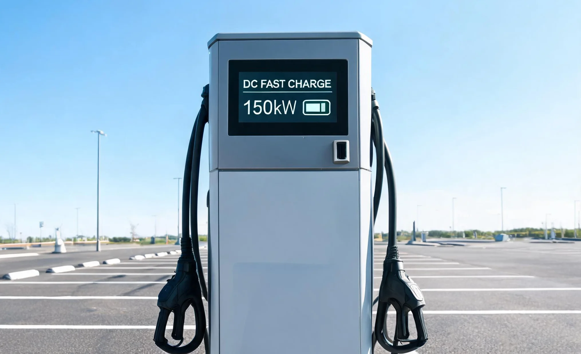
As global electric vehicle sales continue to grow rapidly, the demand for high-power DC fast charging infrastructure has become critical. Infineon’s CoolSiC MOSFET technology represents a significant advancement in charging station power electronics, enabling charging systems up to 350kW that can add 200 kilometers of range in approximately 7 minutes.
CoolSiC MOSFET Product Portfolio for Charging
Infineon offers a comprehensive range of CoolSiC MOSFET products for EV charging applications. The discrete device portfolio includes 650V, 750V, and 1200V CoolSiC MOSFETs, where a single 1200V SiC MOSFET can support 800V DC bus voltage. For higher power charging systems above 50kW, CoolSiC Easy Modules provide the necessary current handling capability. The product range also includes 1700V and 2000V SiC MOSFET modules for ultra-high-voltage charging architectures.
Performance Advantages of CoolSiC Technology
The CoolSiC technology delivers compelling performance benefits for charging station designers. Due to reduced output capacitance (Coss), both conduction and switching losses are reduced by up to 50% compared to silicon alternatives. This enables power density to be doubled, reduces component count by 50% for equivalent silicon solutions, and improves overall system efficiency while reducing cooling requirements. These advantages are particularly significant in high-power charging where thermal management is a primary design challenge.
Complementary Power Semiconductor Technologies
Beyond SiC MOSFETs, Infineon provides CoolMOS superjunction MOSFETs (600V P7 and CFD7 series) for lower power charging stages, IGBT EconoPACK and EconoDUAL modules for AC charging infrastructure, and CoolSiC Schottky diodes for power factor correction circuits. The company’s unique position as a provider of silicon, SiC, and GaN technologies allows charging system designers to select the optimal semiconductor technology for each power conversion stage.
Modular Charging Architecture
Charging stations with capacity exceeding 100kW are typically built using a modular approach, where power sub-units are stacked to achieve the desired total output. This modular design philosophy aligns naturally with Infineon’s power module offerings. The reference design REF-DAB11KIZSICSYS demonstrates an 800V output, 11kW CLLC resonant DC/DC converter stage using IMZ120R030M1H CoolSiC MOSFETs, providing a proven starting point for charging module development.
Bidirectional Charging and V2G Capability
Modern charging infrastructure increasingly supports bidirectional power transfer, enabling vehicle-to-grid (V2G) functionality, home energy backup, and peak load management. CoolSiC MOSFETs’ superior reverse recovery characteristics and low switching losses make them ideal for bidirectional converter topologies. Combined with EiceDRIVER gate drivers, AURIX microcontrollers, AIROC wireless connectivity, and OPTIGA security solutions, Infineon enables complete smart charging systems with grid-interactive capabilities.