1. Ion Implantation
Ion implantation is a critical doping process in semiconductor manufacturing that introduces impurity atoms into a wafer by accelerating ionized dopant species to high energies and directing them at the target material. The following terms are commonly used in this domain:
| Term | Definition |
|---|
| Ion Implanter | A manufacturing tool used to introduce dopant ions into semiconductor wafers through acceleration and implantation. |
| LSS Theory | Lindhand-Scharff-Schiott theory describing the statistical distribution of implanted ions in a target material. |
| Channeling Effect | A phenomenon where implanted ions travel deeper than expected by traveling along open crystal lattice channels. |
| Range Distribution | The statistical spread of the total distance traveled by implanted ions from the wafer surface. |
| Depth Distribution | The concentration profile of dopant atoms as a function of depth below the wafer surface. |
| Projected Range | The average depth measured along the direction of the incident ion beam where implanted ions come to rest. |
| Stopping Power | The rate at which a material dissipates the kinetic energy of incident ions per unit path length. |
2. Annealing and Defects
After ion implantation, the crystal lattice is damaged and dopant atoms are not yet electrically active. Annealing processes repair the lattice and activate dopants. Key terms include:
| Term | Definition |
|---|
| Annealing | A heat treatment process that repairs crystal damage caused by implantation and electrically activates dopant atoms. |
| Activation Energy | The minimum energy required for a physical or chemical process such as dopant diffusion or defect migration to occur. |
| Isothermal Annealing | An annealing process performed at a constant temperature for a specified duration. |
| Laser Annealing | A rapid thermal processing technique using laser energy to melt and recrystallize thin surface layers with minimal bulk heating. |
| Stress-Induced Defect | Crystal defects generated by mechanical or thermal stress during processing, which can degrade device performance. |
| Preferred Orientation | The tendency of polycrystalline films to have grains aligned along specific crystallographic directions. |
3. Photolithography and Patterning
Photolithography transfers patterns from a photomask to a photosensitive material on the wafer surface. It is one of the most critical processes in semiconductor manufacturing, determining minimum feature size and device density.
Mask and Photoresist
| Term | Definition |
|---|
| Photoresist | A light-sensitive material used in lithography to transfer patterns onto a substrate; also called photoresist. |
| Negative Photoresist | A photoresist where the exposed areas become insoluble to the developer, leaving the exposed pattern on the wafer. |
| Positive Photoresist | A photoresist where the exposed areas become soluble to the developer, removing the exposed regions from the wafer. |
| Mask | A patterned plate, typically quartz with chrome patterns, used to transfer circuit designs onto the wafer during lithography. |
| Master Mask | The original high-precision photomask from which working masks are replicated for production use. |
Lithography Processes
| Term | Definition |
|---|
| Photolithography | The process of transferring geometric patterns from a mask to a photosensitive layer on the wafer using light exposure. |
| Electron Beam Lithography | A lithography technique using a focused beam of electrons to write patterns directly onto the resist, enabling very high resolution. |
| Deep-UV Lithography | Photolithography using deep ultraviolet light wavelengths (typically 248nm or 193nm) for finer pattern resolution. |
| X-ray Lithography | A lithography technique using X-rays to achieve sub-micron resolution through shorter wavelength radiation. |
| Mask Alignment | The process of precisely positioning a photomask over previously patterned features on the wafer. |
4. Etching Processes
Etching removes material from the wafer surface according to the patterned resist layer. Both wet and dry etching techniques are used in semiconductor manufacturing, with dry etching dominating advanced technology nodes due to its anisotropic profile control.
| Term | Definition |
|---|
| Dry Etching | An etching process using plasma or reactive gases instead of liquid chemicals, enabling highly directional material removal. |
| Reactive Ion Etching (RIE) | A dry etching technique combining chemical reaction and physical ion bombardment to achieve anisotropic etch profiles. |
| Isotropic Etching | Etching that proceeds at equal rates in all directions, typically associated with wet chemical etching processes. |
| Anisotropic Etching | Etching that proceeds faster in the vertical direction than horizontally, producing straight sidewall profiles critical for small features. |
| Plasma Etching | A form of dry etching that uses ionized gas (plasma) to chemically and physically remove material from the wafer surface. |
| Undercutting | The lateral etching of material beneath a mask or resist layer, which can degrade pattern fidelity and feature size control. |
5. Metallization and Interconnection
Metallization deposits conductive metal layers that connect individual devices into functional circuits. Multi-level interconnect schemes stack multiple metal layers separated by dielectric materials.
| Term | Definition |
|---|
| Metallization | The process of depositing and patterning metal films to form electrical connections between devices and circuit components. |
| Interconnection | The wiring system (metal lines and vias) that electrically connects transistors and components within an integrated circuit. |
| Multilevel Metallization | A wiring scheme using multiple stacked metal layers separated by dielectric materials to achieve high-density circuit routing. |
| Electromigration | The gradual transport of metal atoms caused by high current density, which can lead to open or short circuits in interconnect lines. |
| Passivation | A protective dielectric layer deposited over the finished device to shield it from moisture, contamination, and mechanical damage. |
6. Packaging and Assembly
Packaging encloses the finished semiconductor die in a protective housing and provides electrical connections to the outside world. Packaging technologies range from traditional through-hole packages to advanced flip-chip and system-in-package solutions.
| Term | Definition |
|---|
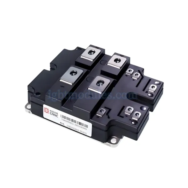
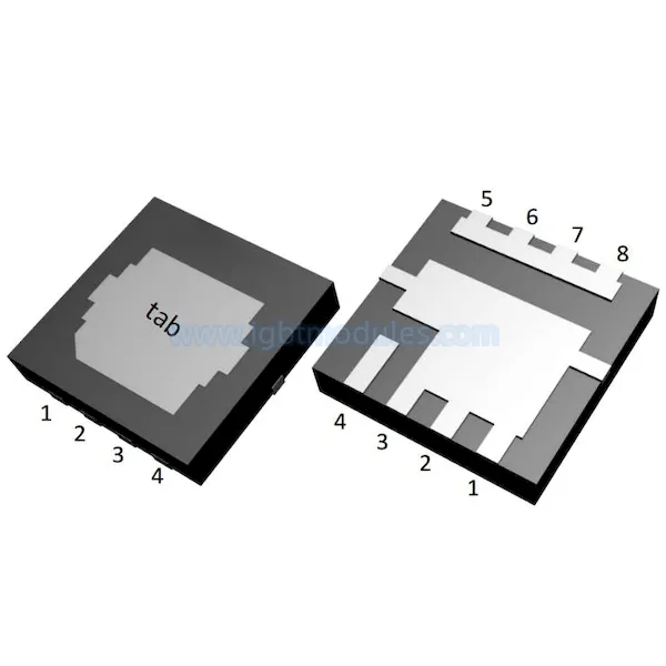
| Packaging | The process of enclosing a semiconductor die in a protective package, providing electrical connections, thermal management, and physical protection. |
| Wire Bonding | A method of making electrical connections between a chip and its package using thin metal wires (typically gold, aluminum, or copper). |
| Ball Bonding | A wire bonding technique that forms a ball at the end of the wire through electrical discharge, creating a round contact pad on the chip. |
| Tape Automated Bonding (TAB) | A packaging technology that uses a flexible polymer tape with pre-fabricated metal traces for high-density chip interconnection. |
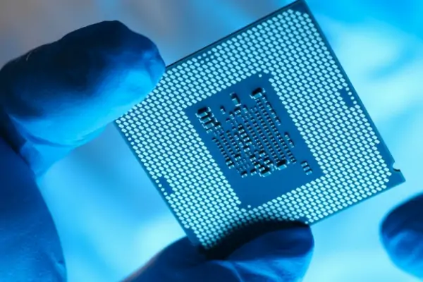
| Flip Chip | A packaging technique where the chip is mounted face-down, connecting directly to the substrate through solder bumps for high density and performance. |
| Ceramic Package | A semiconductor package made from ceramic materials, offering excellent hermeticity, thermal conductivity, and high-temperature performance. |
7. Device Physics Fundamentals
Understanding semiconductor device behavior requires familiarity with basic physics concepts related to energy bands, charge carriers, and junction phenomena. Below are fundamental terms from the A-to-Z microelectronics dictionary.
| Term | Definition |
|---|
| Band Gap | The energy difference between the valence band and conduction band in a semiconductor material; determines its electrical conductivity properties. |
| Avalanche Breakdown | A breakdown mechanism where high electric fields accelerate charge carriers to energies sufficient to create additional electron-hole pairs through impact ionization. |
| Bipolar Device | A semiconductor device that uses both electrons and holes as charge carriers for conduction, such as bipolar junction transistors (BJT) and IGBTs. |
| Doping | The intentional introduction of impurity atoms into a semiconductor material to modify its electrical conductivity and type (n-type or p-type). |
| Depletion Region | The region near a p-n junction where mobile charge carriers have been swept away, leaving ionized dopant atoms and creating a built-in electric field. |